High Precision Lapping and Polishing Equipments
Discover our range of high-precision equipment designed for the semiconductor industry
Multi Stations,Semi-auto Wafer bonder for semiconductor wafer bonding
View Details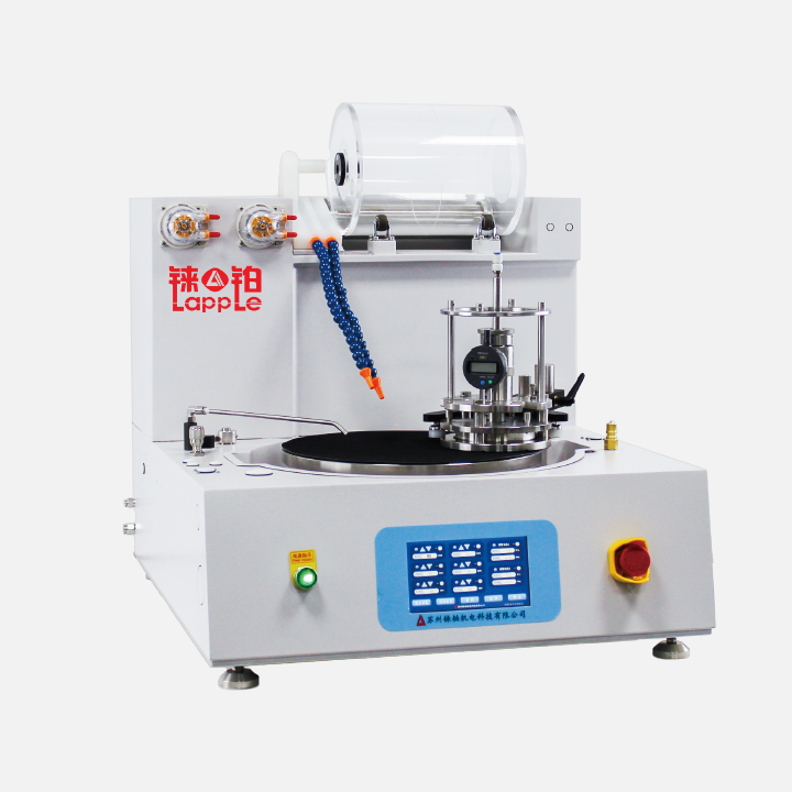
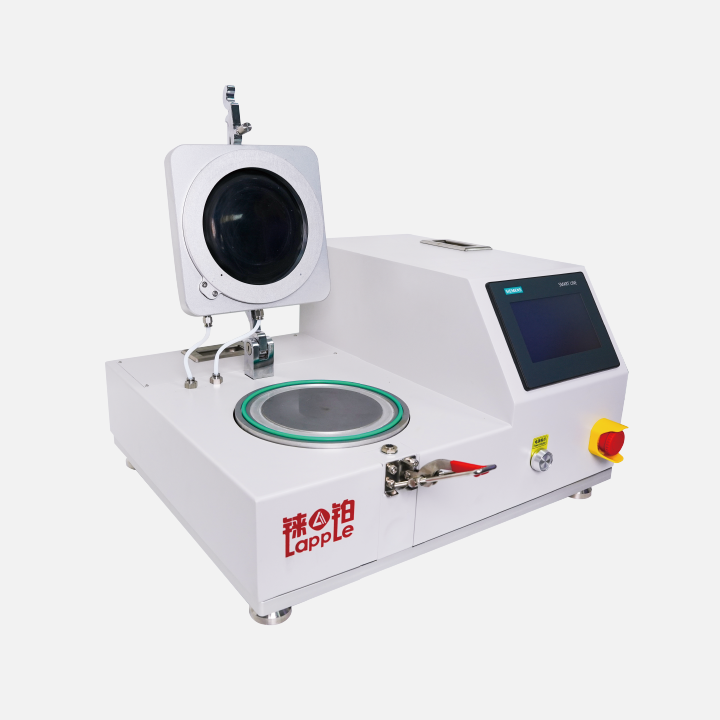
High Precision Lapping and Polishing Machine for wafers,chips,fibers,etc
View Details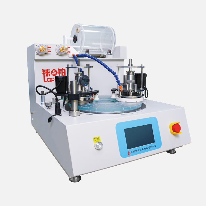
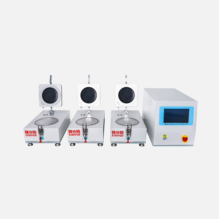
High Precision Lapping and Polishing Machine for wafers,chips,fibers,etc
View Details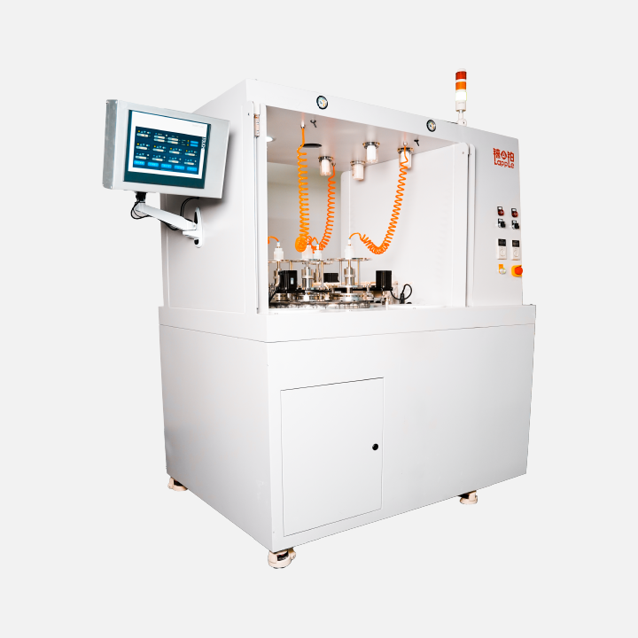
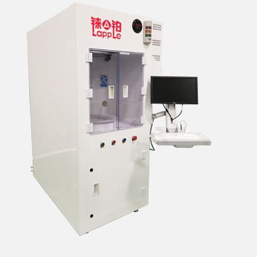
High Precision Lapping and Polishing Machine for wafers,chips,fibers,etc
View Details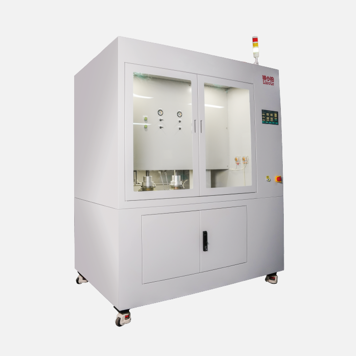
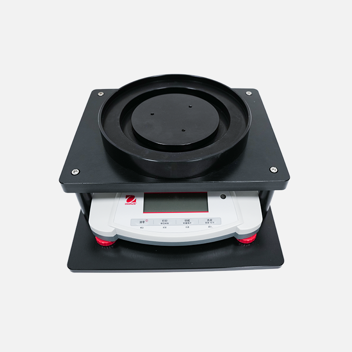
For load measurement of precision lapping and polishing jigs
View Details
For III-V materials,InP and GaAs wafers and chips precision polishing.
View Details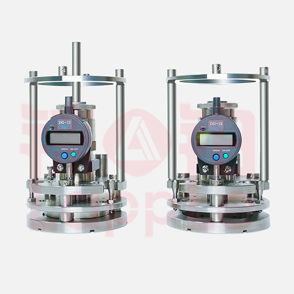
High-quality and High Precision Lapping and Polishing Jig.
View Details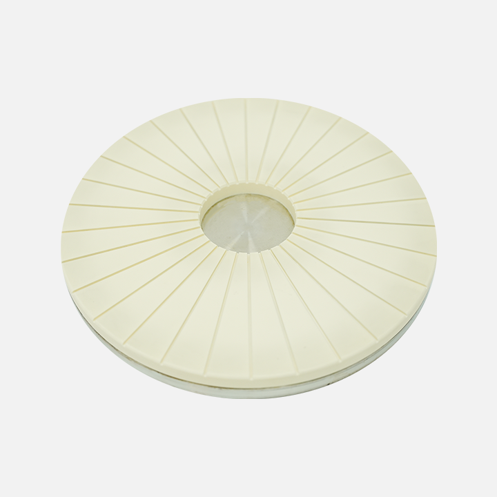
High Precision Lapping and Polishing Plates,different materials,Cast Iron,Ceramic,Glass,Copper.....
View Details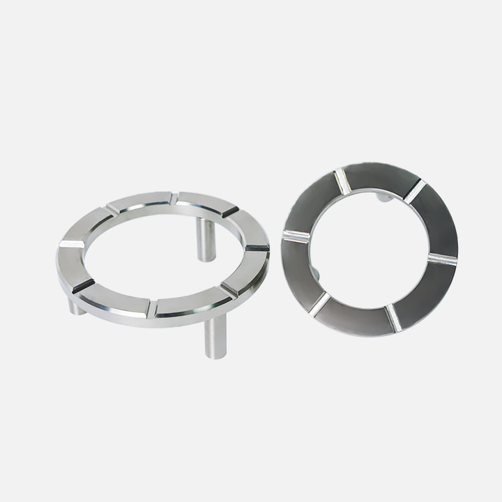
Driving ring for lapping and polishing Jig,different materials,SS,Ceramic,Glass.....
View Details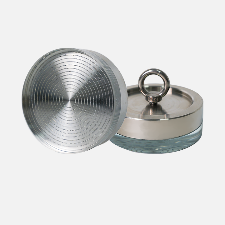
Test Blocks for Lapping Plates for lapping plates,different materials,Cast Iron,Ceramic,Glass.....
View Details