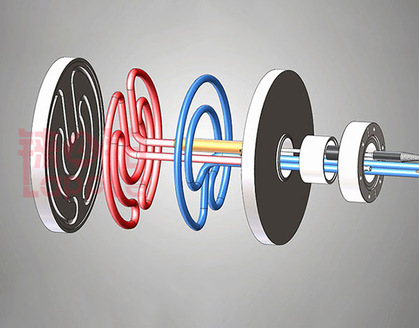
High Precision Lapping and Polishing Equipments
Precision surface preparation is paramount in semiconductor manufacturing. Our specialized Lapple lapping and polishing driving ring are engineered to meet the extreme demands of processing semiconductor wafers (Silicon, SiC, GaAs, GaN, InP, Sapphire,MCT,CZT,InSb....) and critical components. They provide the essential foundation for achieving ultra-flat, damage-free surfaces with nanometer-level precision required for subsequent lithography, deposition, and inspection stages. Selection of the optimal plate material and groove pattern is critical based on the substrate material, wafer size (e.g., 150mm, 200mm), process stage (rough lapping, fine lapping, polishing), and desired surface finish.
Manufactured to micron flatness specifications. Essential for achieving uniform material removal.
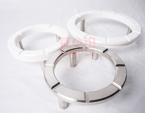
Grooves are critical for slurry distribution, debris removal, heat dissipation, and pressure control.
Engineered to minimize subsurface damage, micro-cracks, and scratches during material removal, preserving wafer integrity and device yield.
High-quality materials and precision manufacturing ensure long service life and consistent performance batch-to-batch, reducing consumable costs and process variability.
| Materials | Stainless Steel | Glass | Ceramic | Diamond | Others customized |
|---|---|---|---|---|---|
Ring ID |
85mm | 114mm | 165mm | 215mm | Special sizes can be customized. |
Ring TTV |
+/-2um | +/-2um | +/-3um | +/-3um | Better TTV also can be reached. |
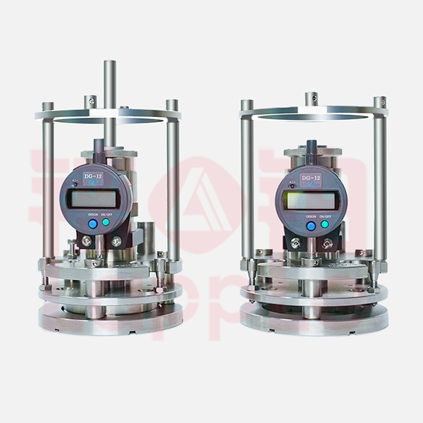
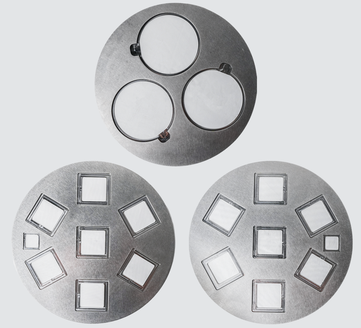
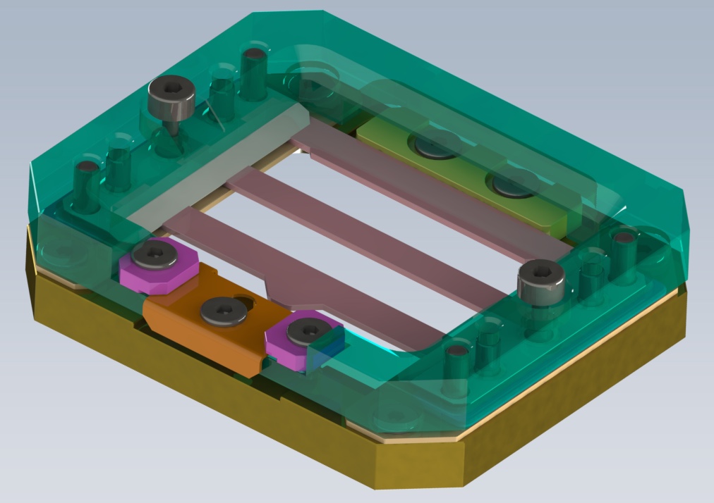
High-quality and High Precision Lapping and Polishing Jig.
View Details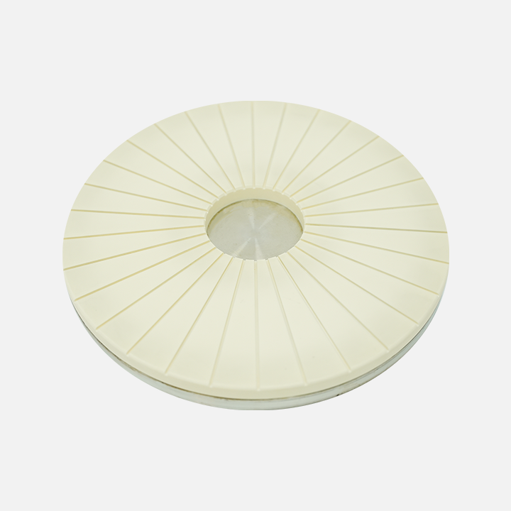
High Precision Lapping and Polishing Plates,different materials,Cast Iron,Ceramic,Glass,Copper.....
View Details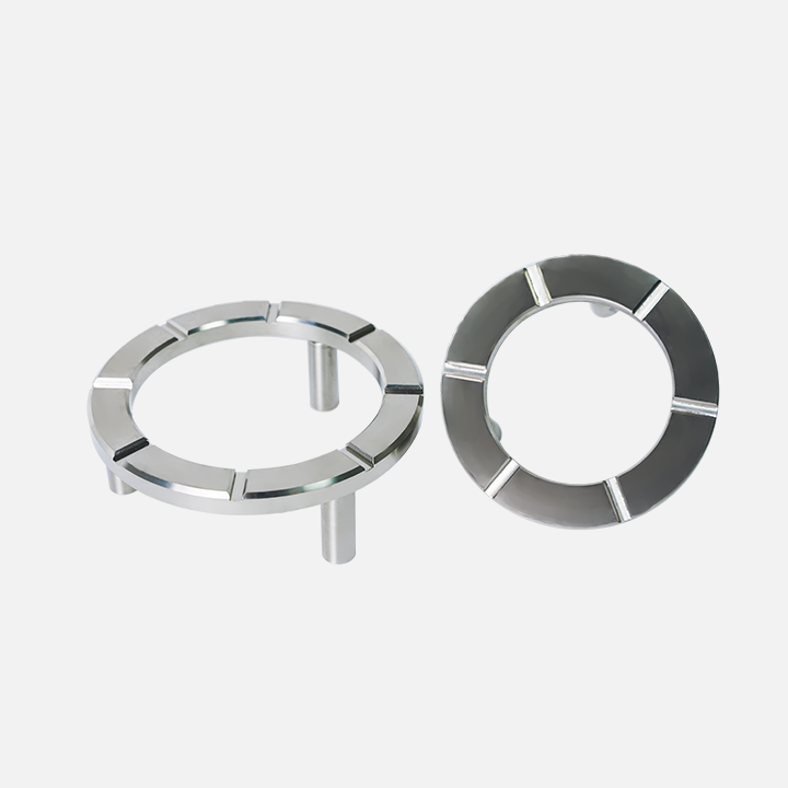
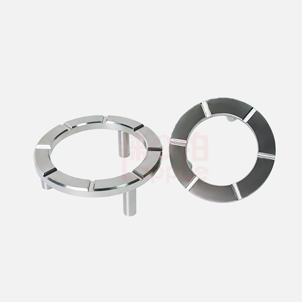
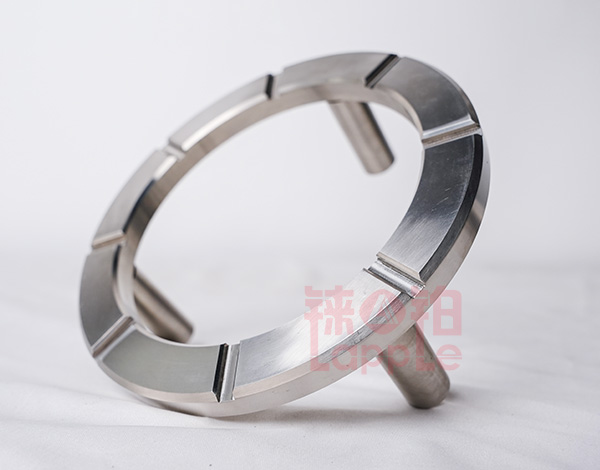
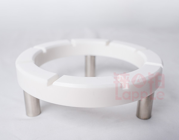
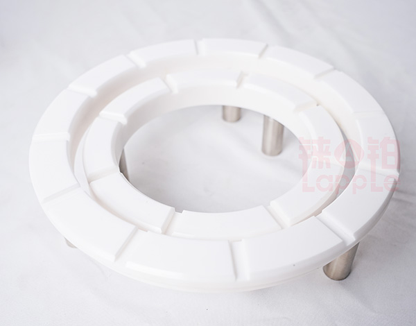
Driving ring for lapping and polishing Jig,different materials,SS,Ceramic,Glass.....
View Details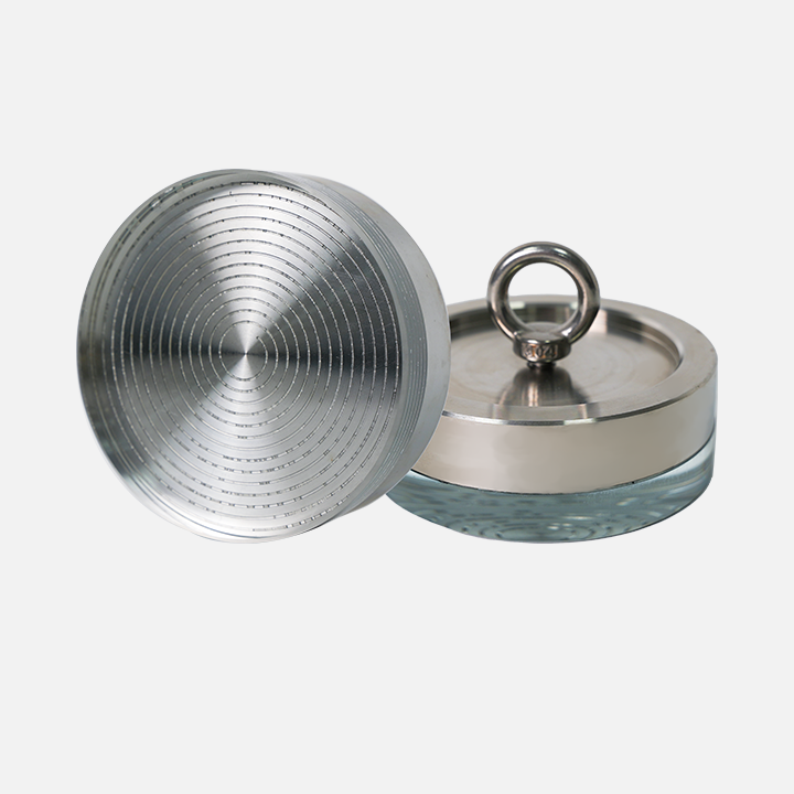
Conditioners/Test Blocks for Lapping and Polishing plates,different materials,Cast Iron,Ceramic,Glass.....
View Details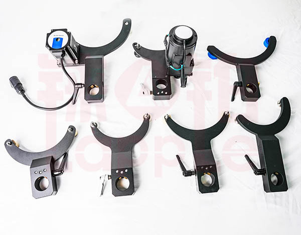
Bar jig for bar stacker machine,such as Opto and Daitron bar stacker system.
View Details