High Precision Lapping and Polishing Equipments
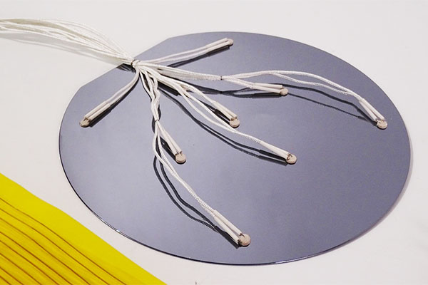
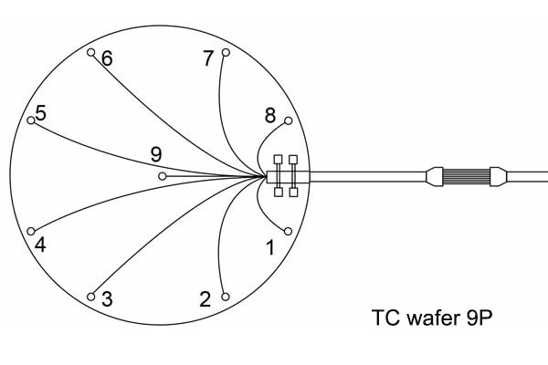
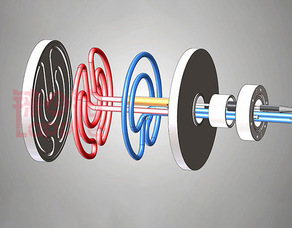
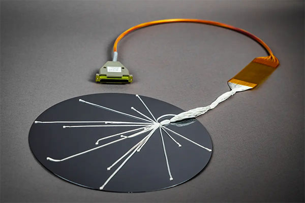
A TC Wafer is a customizable, instrumented wafer with embedded thermocouples designed for accurate, real-time, in-situ temperature profiling and transient monitoring of semiconductor wafers during processing. It is a critical tool for gaining process confidence, ensuring equipment health, improving uniformity, troubleshooting temperature issues, and ultimately enhancing yield and uptime in semiconductor manufacturing.
It is widely used to monitor and validate the performance of critical semiconductor manufacturing equipment (Etch, PVD, CVD, RTP, Bonders,Hotplates, Ovens, Reflow, etc.).
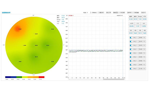
Enables measurement of the actual temperature experienced by the wafer inside the process chamber, leading to greater process control and reliability.
Helps identify root causes of temperature deviations between equipment sets or within a single tool faster.
Reveals process temperature uniformity across the wafer.
Contributes to increased uptime of manufacturing equipment by enabling better process control and faster diagnostics.
| Sensor Type | Wafer Size | Substrate | Number of sensors | Wire termination | Temperature Range |
|---|---|---|---|---|---|
| K Type | 3~12" | Silicon,Sapphire,metal | 1~20 | Min Plug/D-sub | RT~1000℃ |
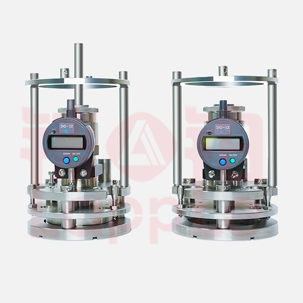
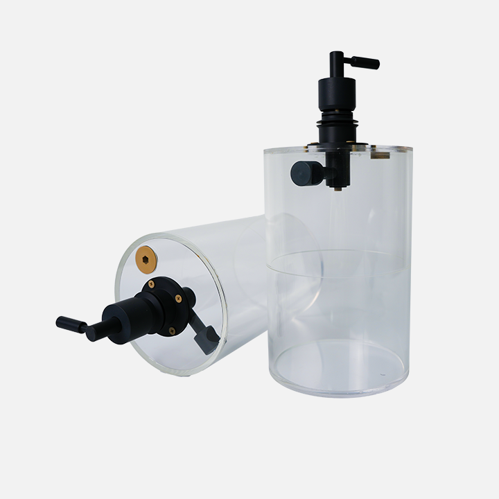
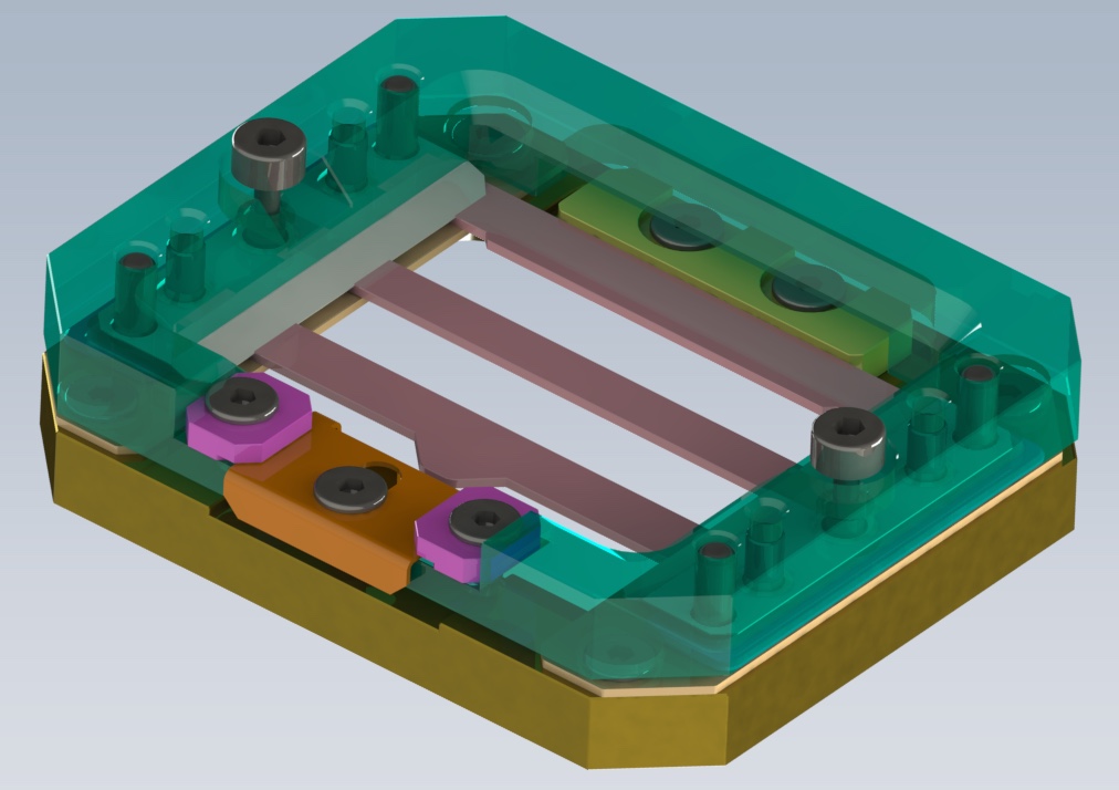
High-quality and High Precision Lapping and Polishing Jig.
View Details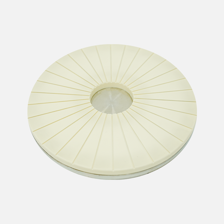
High Precision Lapping and Polishing Plates,different materials,Cast Iron,Ceramic,Glass,Copper.....
View Details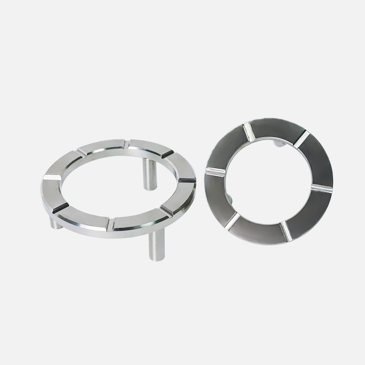
Driving ring for lapping and polishing Jig,different materials,SS,Ceramic,Glass.....
View Details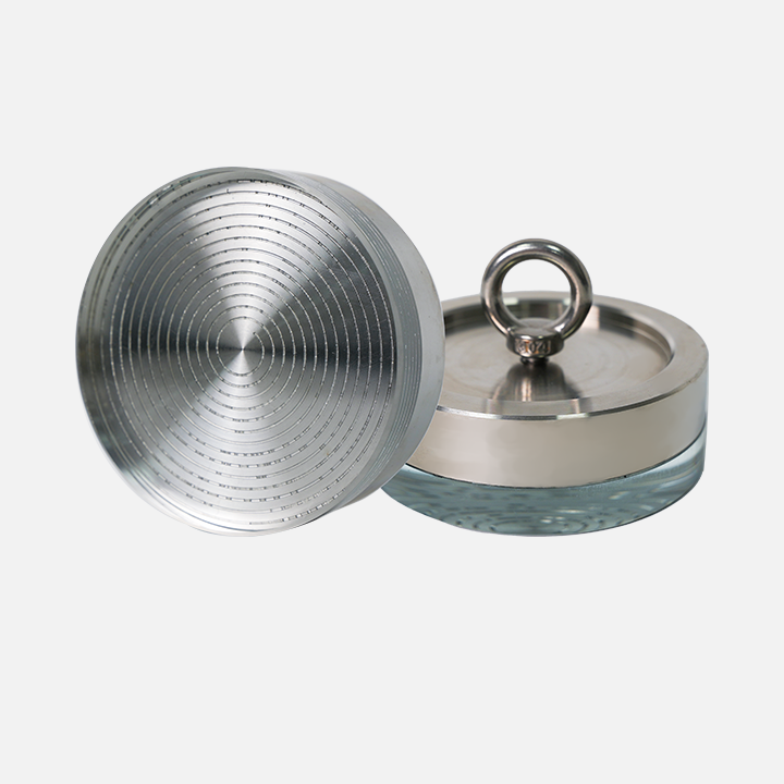
Conditioners/Test Blocks for Lapping and Polishing plates,different materials,Cast Iron,Ceramic,Glass.....
View Details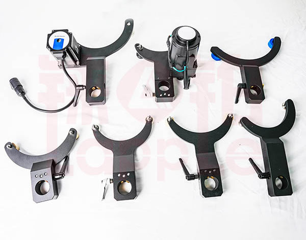

Bar jig for bar stacker machine,such as Opto and Daitron bar stacker system.
View Details