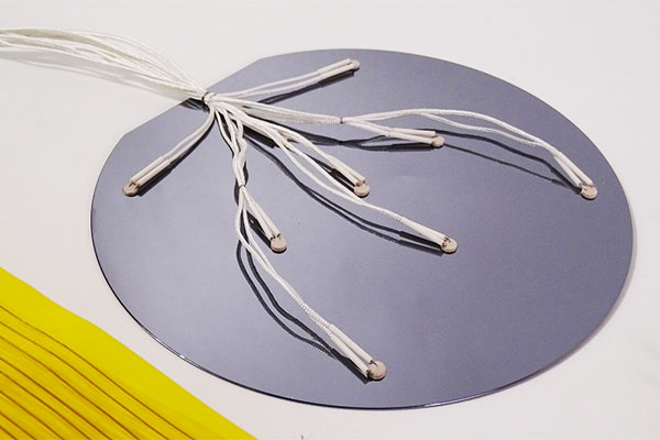
High Precision Lapping and Polishing Equipments
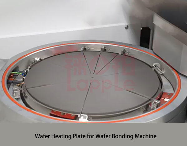
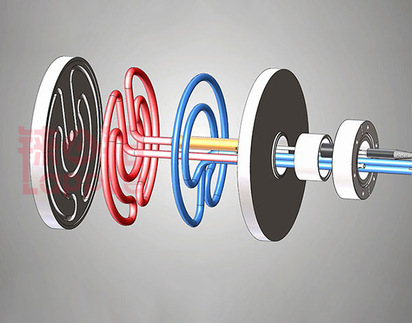
Wafer heaters are high-precision thermal management components essential for semiconductor fabrication processes requiring extreme temperature uniformity, stability, and repeatability. Engineered specifically for demanding environments like Wafer Bonding, Chemical Vapor Deposition (CVD), Physical Vapor Deposition (PVD), and Atomic Layer Deposition (ALD), these heaters provide controlled, uniform heating to semiconductor wafers mounted on susceptors, chucks, or pedestals within process chambers. Constructed from advanced materials like aluminum alloys or high-purity technical ceramics, they integrate efficient heating elements and often feature embedded sensors for real-time temperature feedback, ensuring optimal process control under vacuum or controlled atmospheres.
Semiconductor and Wafer Processing Solutions
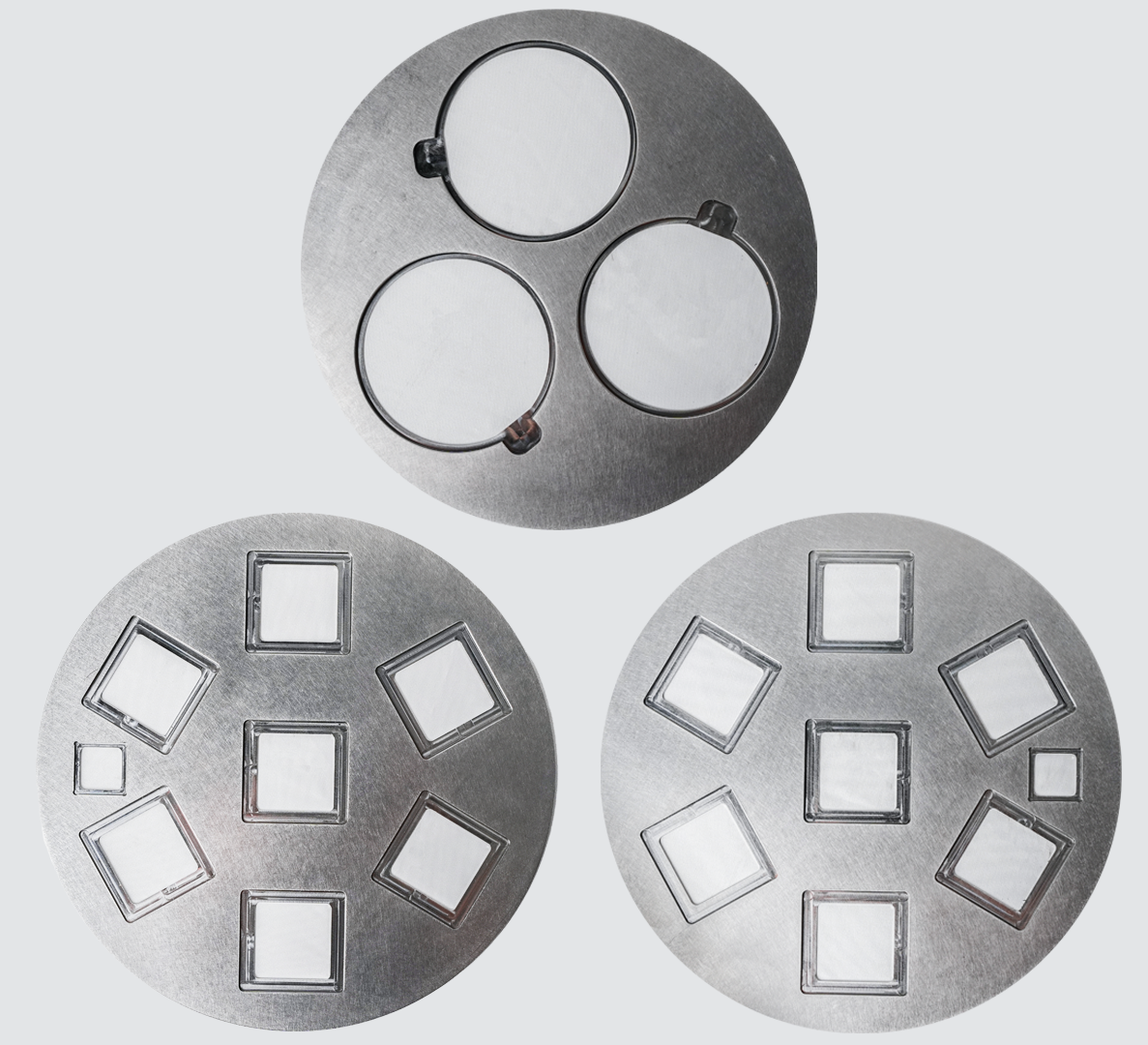
Lapple designs and manufactures critical in-chamber heating and cooling devices, as well as custom-engineered thermal devices for a variety of Semiconductor and Wafer Processing applications. Lapple offers a diverse range of customized heaters to meet the varied needs of your requirements. Lapple utilizes precision machining and measurement equipment to uphold the precision of product specifications and quality standards.
One of the core technologies of Lapple is the complete development and production of innovative heaters used in Bonder,CVD & PVD Process. We possess the capability to develop and provide customized solutions for various customer needs in addition to a wide range of optimal standard products. Lapple takes great pride in its familiarity with materials, enabling rapid design and proposal of any customized model to meet full range of specific temperature requirements. With over 15 years of experience in the field of heaters, technical expertise stands as crucial advantage of Lapple.
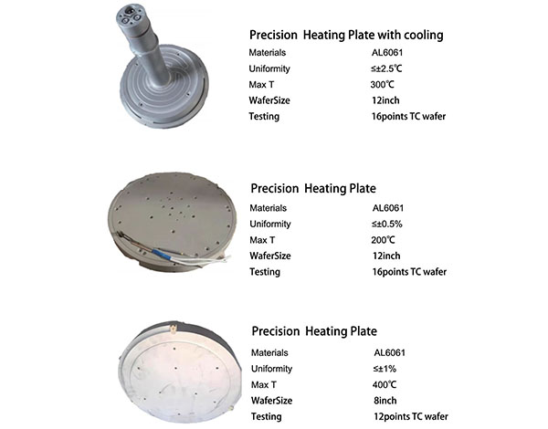
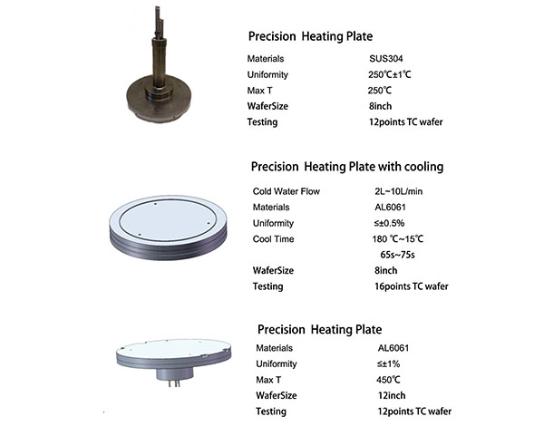
Achieves ultra-low temperature gradients (±1°C to ±5°C typical across the wafer surface). Minimizes wafer stress and defects.Critical for uniform film deposition/etch rates/ successful wafer bonding.
Low thermal mass designs enable fast ramp-up and cool-down rates, improving throughput.Maintains setpoint temperatures with minimal fluctuation, ensuring process repeatability.
High thermal conductivity for efficient heat spreading.Excellent mechanical strength and stability for wafer bonding pressure.Often anodized for corrosion resistance.
Tailored to fit specific tool chamber geometries and wafer sizes .Optimized power density and wiring configurations (e.g., multi-zone heating).
| Materials | T Max | Process | Chemical/Plasma Resist | Pressure Handling | Thermal Conductivity |
|---|---|---|---|---|---|
| Aluminum Alloys | <~450°C | Wafer Bonding, PVD (Moderate Temp) | Moderate (Requires Anodizing) | Limited | Very High |
| Al2O3 | >500°C (Al₂O₃) | CVD, ALD, High-Temp PVD | Excellent (Inherent Resistance) | Excellent/brittle | Moderate |
| AlN, SiC | >800°C (SiC) | CVD, ALD, High-Temp PVD | Excellent (Inherent Resistance) | Excellent/brittle | High |
| Stainless Steel (SS) | >450°C | Wafer Bonding(high pressure) | Good | Excellent | Low |
High-quality and High Precision Lapping and Polishing Jig.
View Details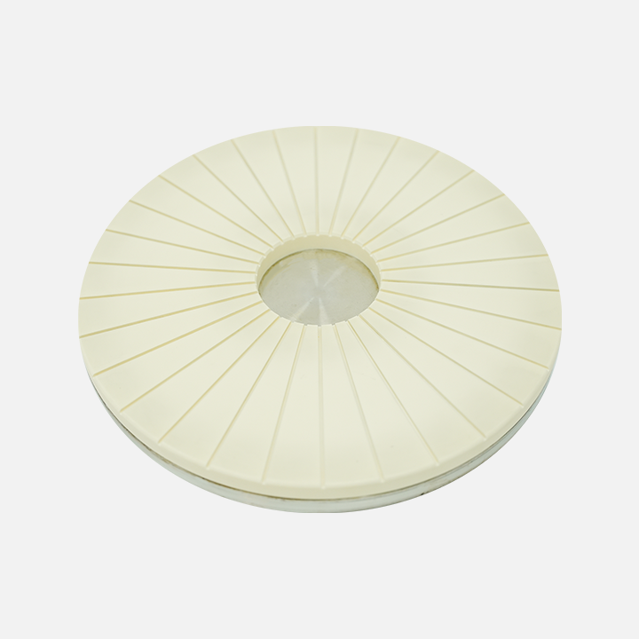
High Precision Lapping and Polishing Plates,different materials,Cast Iron,Ceramic,Glass,Copper.....
View Details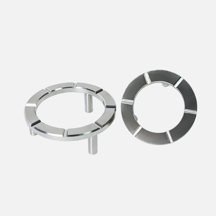
Driving ring for lapping and polishing Jig,different materials,SS,Ceramic,Glass.....
View Details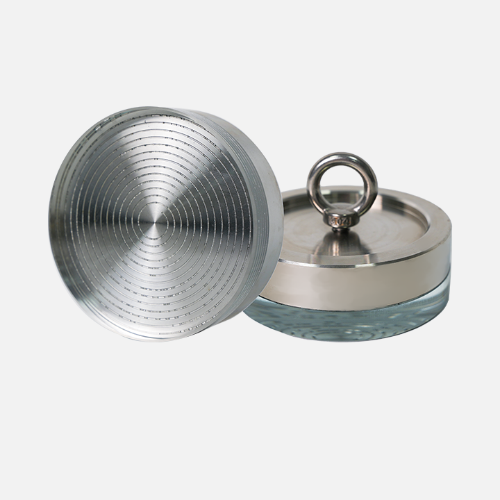
Conditioners/Test Blocks for Lapping and Polishing plates,different materials,Cast Iron,Ceramic,Glass.....
View Details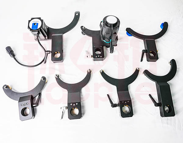
Bar jig for bar stacker machine,such as Opto and Daitron bar stacker system.
View Details