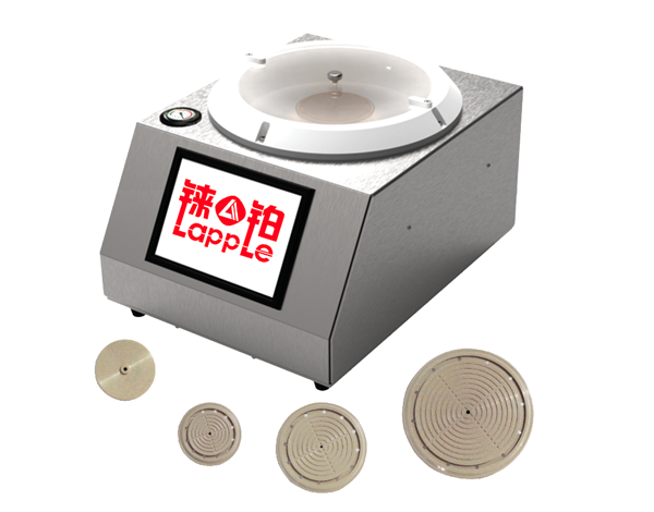
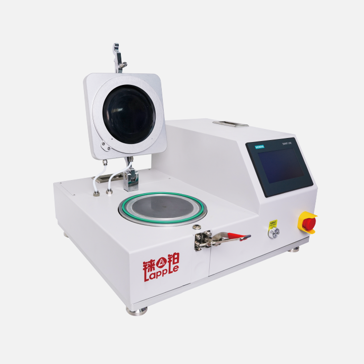
High Precision Lapping and Polishing Equipments
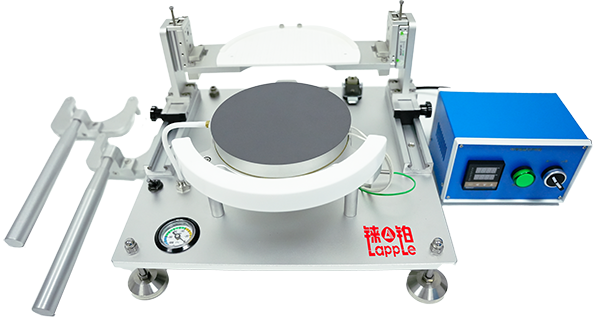
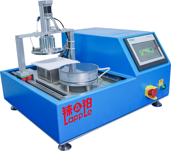
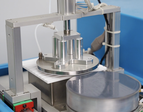
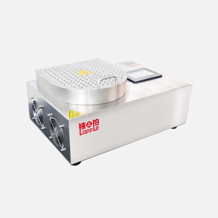
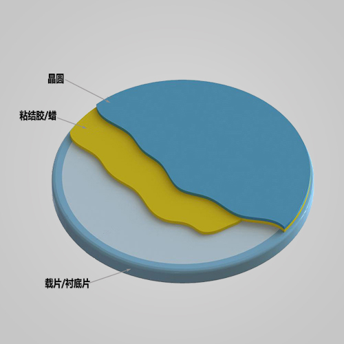
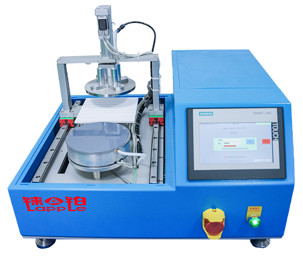
In the wafer thinning and polishing process, the wafer needs to be bonded to the substrate using temporary bonding materials. After the wafer thinning and polishing are completed, the wafer and substrate need to be separated. The DB-041 is an automatic debonder which can automatically separates the wafer from the substrate. TP001 is a desktop manual wafer debonder,very compact and convenvient. For wafer debonding after thinning or polishing process.Wafer size up to 6" ,8" version can be customized,Easy operation. These two machines are our debonding solution designed for advanced semiconductor manufacturing. Designed for InP,GaAs wafers debonding,also suitable for Silicon,GaN,SiC,Diamond,Ceramic etc. With its innovative debonding capabilities, it ensures excellent debonding and no damage for your materials.
Very compact and convenient.
After debonding wafer no damage
Excellent temperature uniformity,temperature up to 300degree
Sliding speed multi steps control to ensure no damage to the wafer
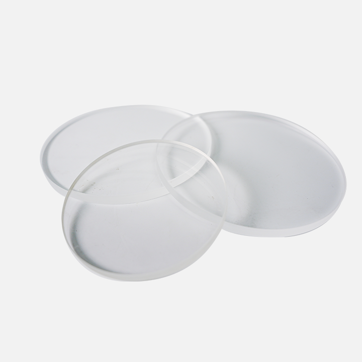
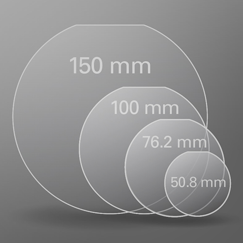
| Wafer Size | up to 150mm,large size can be customizable |
|---|---|
| Functions | Heating,vacuum,sliding(by hand/by machine) |
| Pressure | -0.8Mpa(vacuum) |
| Temperature Range | Room Temp to 300°C |
| Throughput | Depends on the process |
| Tools | Porous plate included, hand-operated tools(manual version) |
| Power Requirements | 220V, 10A |
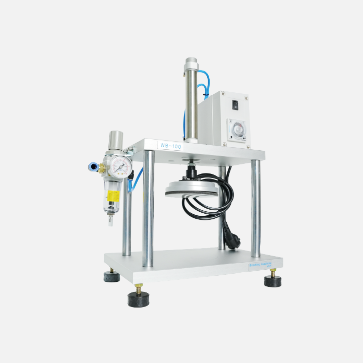
Multi Stations,Semi-auto Wafer bonder for semiconductor wafer bonding
View Details