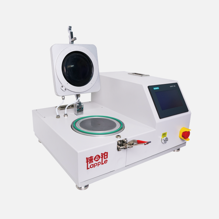
High Precision Lapping and Polishing Equipments
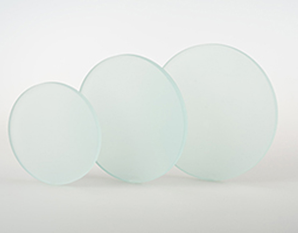
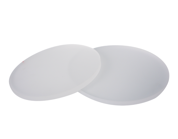
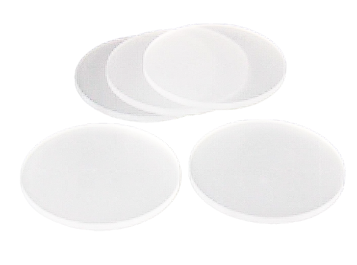
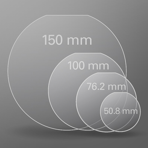
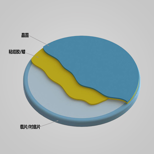
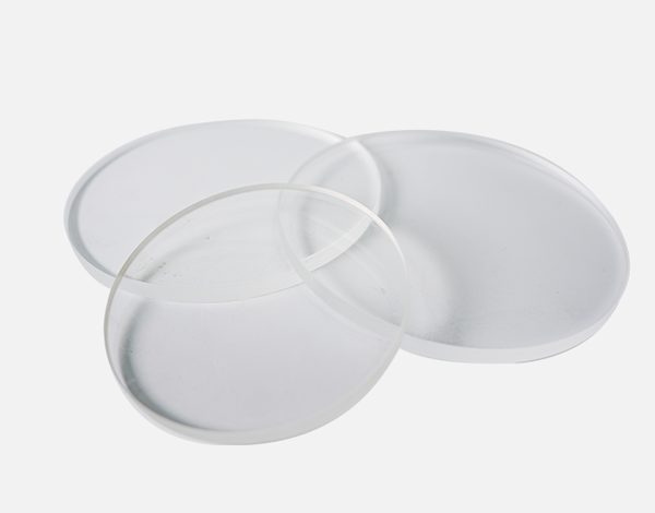
Glass and Quartz substrates, For substrates 112mm in diameter,thickness about 6mm,TTV <=2um;For substrates 160mm in diameter,thickness about 8mm,TTV <=4um;For substrates 200mm in diameter,thickness about 10mm,TTV <=6um; Double sides lapped. Specially designed for temporary bonding of semiconductor materials such as GaAs, InP, Si, etc.,They can be customized according to requirements. Supports double-sided polishing and double-sided lapping, with extremely high flatness to ensure high-precision processing. Wear resistant and durable, with excellent transparency and resistance to chemical corrosion and scratching. It can be reused many times and is economical and practical. Specially suitable for precision processing of semiconductor materials such as GaAs, InP, Si, etc.
105mm,112mm,160mm,200mm,315mm,other sizes can be customized according to your requirements.
6mm,8mm,10mm,can be customized according to your requirements.
Double-sided lapped,very good TTV,high temperature resistant
Glass,Quartz,other specified materials
| Substrate Size | Up to 315mm in diameter |
|---|---|
| Thickness | 6mm~20mm |
| TTV | 2um,4um,6um,8um,10um,15um for different diameters |
| Temperature | Can be used at high temperature. |
| Chemical resistant | Resistance to chemical corrosion and scratching |
| Materials | Glass,Quartz,other specified materials |
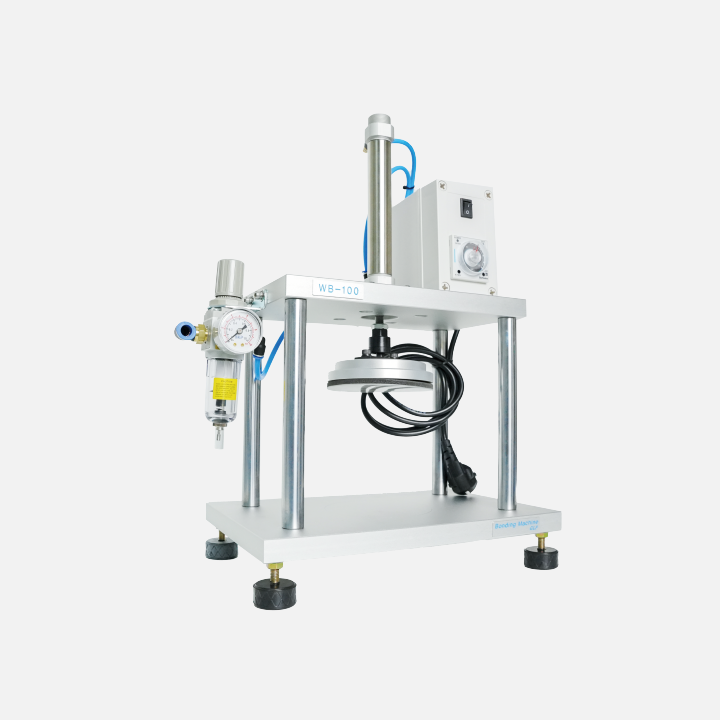
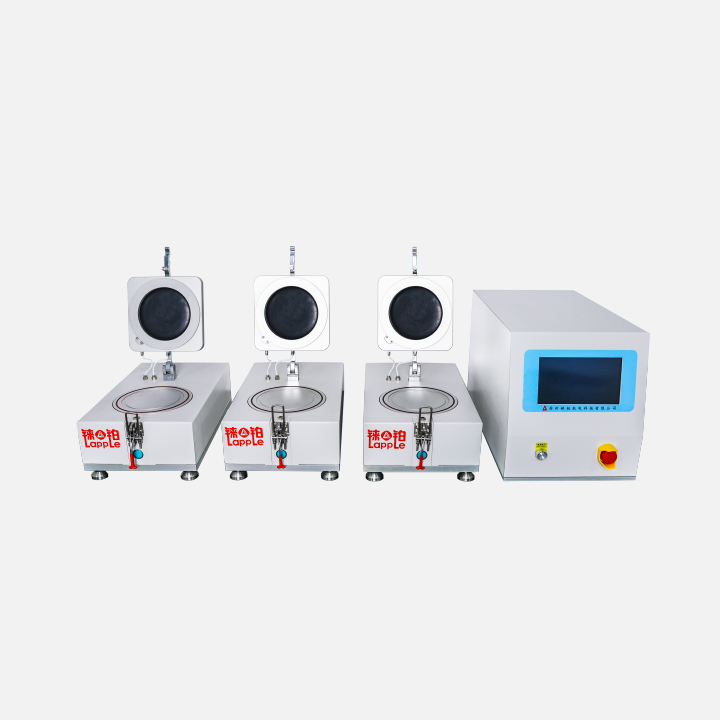
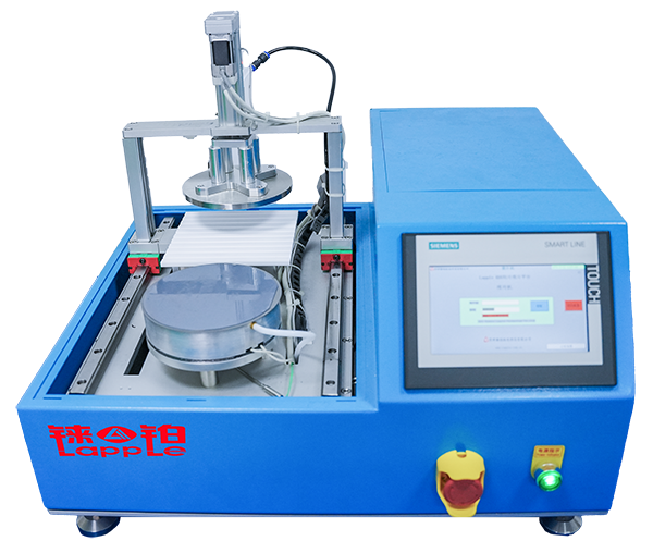
Multi Stations,Semi-auto Wafer bonder for semiconductor wafer bonding
View Details