Advanced Lapping and Polishing Solutions for Semiconductor Industry
Our advanced wafer temporary bonding solution delivers superior, reliable temporary wafer bonding essential for demanding thin-wafer handling processes.
Engineered for maximum flexibility across diverse semiconductor applications, the solution combines advanced process control with broad material compatibility to address critical thin-wafer challenges:
Vacuum-Assisted Degassing Chamber:Active volatile removal prevents bubble formation and ensures chemical compatibility with sensitive device layers.
Multi-Material Wax Compatibility,precisely matched to: Substrate materials,Final thickness requirements (down to ≤50μm) and Downstream processes (Lapping,Polishing, TSV, Debonding).

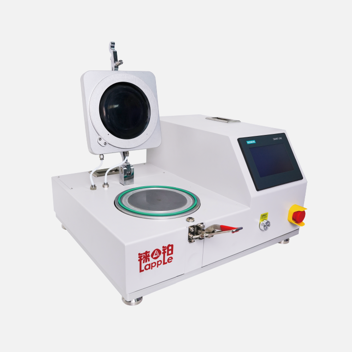
Lapple wafer bonder Demo Video,for wafer temporary bonding with substrates.
After bonding no bubble no damage,and wax layer very uniform.
Easy to operate with stored process, faster processing times while maintaining superior bonding quality and uniformity.
Intelligent process monitoring and adaptive control ensure consistent results with minimal operator intervention.
Complete wafer bonding solution for ultra-thin wafer processing, ideal for advanced packaging applications.
View Details

Contact our team to discuss how our precision lapping and polishing solutions can enhance your production quality and efficiency.